US 11,719,871 B2
Polarizer, display panel including the same and method of manufacturing the same
Kang-Soo Han, Seoul (KR); Eun-Jung Kim, Suwon-si (KR); Gug-Rae Jo, Asan-si (KR); and Hyung-Bin Cho, Seongnam-si (KR)
Assigned to SAMSUNG DISPLAY CO., LTD., Yongin-si (KR)
Filed by SAMSUNG DISPLAY CO, LTD., Yongin-si (KR)
Filed on Aug. 13, 2021, as Appl. No. 17/401,448.
Application 17/401,448 is a division of application No. 16/261,722, filed on Jan. 30, 2019, granted, now 11,112,549.
Application 16/261,722 is a division of application No. 14/799,804, filed on Jul. 15, 2015, granted, now 10,222,527, issued on Mar. 5, 2019.
Claims priority of application No. 10-2014-0148420 (KR), filed on Oct. 29, 2014.
Prior Publication US 2021/0373221 A1, Dec. 2, 2021
Int. Cl. G02B 5/30 (2006.01); G02F 1/1335 (2006.01)
CPC G02B 5/3058 (2013.01) [G02F 1/133548 (2021.01)] 10 Claims
OG exemplary drawing
 
1. A display panel, comprising:
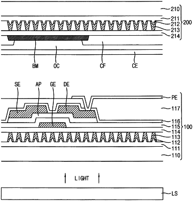
a thin film transistor;
a buffer member including a plurality of protrusions, wherein each protrusion is protruded from an upper surface of the buffer member and the protrusions cause the buffer member to have a corrugated surface;
a plurality of metal lines disposed over the corrugated surface of the buffer member, wherein each protrusion is enclosed by a respective metal line, and wherein two adjacent metal lines expose a part of the upper surface of the buffer member therebetween; and
a protective layer interposed between a gate electrode of the thin film transistor and the metal lines,
wherein the gate electrode overlaps the at least two adjacent metal lines.