| CPC G01T 1/026 (2013.01) [H01L 31/0312 (2013.01); H01L 31/117 (2013.01); H01L 31/1812 (2013.01)] | 16 Claims |
|
1. A detector for ionizing radiation, configured as a telescopic detector with at least two detector stages, the detector comprising a monolithic body formed by a multilayer planar structure which comprises:
an upper face comprising an active area of the detector and a lower face, opposite to the upper face in a vertical direction (Z-Z) of thickness of the detector;
a substrate consisting of SiC, adjacent to the lower face in the vertical direction (Z-Z);
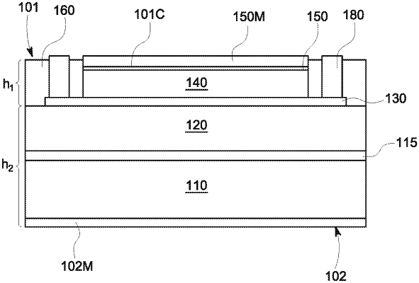
a first epitaxial layer that is a n− or p− type epitaxial layer (120, 420), arranged between the substrate and the upper face and having a thickness of between 10 and 100 μm, with a dopant concentration of about 5-8·1013/cm3;
a second epitaxial layer that is a p+ or n+ type epitaxial layer (130, 430), arranged on top of the first epitaxial layer and having a thickness smaller than the thickness of the first epitaxial layer, with a dopant concentration of about 1018-1019/cm3;
a third epitaxial layer that is a n− or p− type epitaxial layer (140, 440), arranged on the second epitaxial layer and having a thickness of between 2 and 10 μm and dopant concentration of about 5-8·1013/cm3; and
a fourth epitaxial layer that is a n+ or p+ type epitaxial layer (150, 450), with a thickness of 0.1 to 1 μm, and dopant concentration of about 1018/cm3, a top surface of the fourth epitaxial layer forming the active area of the detector, the multilayer planar structure resulting in at least one first detector stage defined between a cathode and an anode and comprising at least the fourth epitaxial layer (150, 450), the third epitaxial layer (140, 440) and the second epitaxial layer (130, 430) arranged so as to form a p-n or n-p junction, and a second detector stage arranged in sequence with the first detector stage in the vertical direction (Z-Z), defined between a cathode and an anode and comprising at least the second epitaxial layer (130, 430), the first epitaxial layer (120, 420) and the substrate (110) arranged so as to form an n-p or p-n junction,
wherein the first epitaxial layer (120) is of a n− type, the second epitaxial layer (130) is of the p+ type, the third epitaxial layer (140) is of the n− type, and the fourth epitaxial layer (150) is of the n+ type, and wherein the cathode of the first detector stage is in contact with the fourth n+ type epitaxial layer (150) and the anode of the first detector stage is in contact with the second p+ epitaxial layer (130), and the cathode of the second detector stage is in contact with the substrate and the anode of the second detector stage is in contact with the second p+ type epitaxial layer (130), or the first epitaxial layer (420) is of p− type, the second epitaxial layer (430) is of n+ type, the third epitaxial layer (440) is of p− type, and the fourth epitaxial layer (450) is of p+ type, and wherein the anode of the first detector stage is in contact with the fourth p+ type epitaxial layer (450) and the cathode of the first detector stage is in contact with the second n+ type epitaxial layer (430), and the anode of the second detector stage is in contact with the substrate (110) and the cathode of the second detector stage is in contact with the second n+ type epitaxial layer (430).
|