| CPC G01S 17/10 (2013.01) [G01S 7/481 (2013.01); G01S 7/484 (2013.01); G01S 7/4811 (2013.01); G01S 7/4863 (2013.01); G02B 7/003 (2013.01); H01L 31/107 (2013.01); G02B 2006/12083 (2013.01); G02B 2006/12102 (2013.01)] | 12 Claims |
|
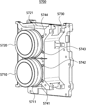
1. A light detection and ranging (LiDAR) device comprising:
a laser emitting chip configured to emit laser;
a laser detecting chip configured to detect laser;
an emitting optic module configured to guide laser generated from the laser emitting chip to the outside of the LiDAR device;
a detecting optic module configured to guide laser received from the outside of the LiDAR device to the laser detecting chip;
an emitting optic holder located between the laser emitting chip and the emitting optic module; and
an at least one emitting optic fixer located between the emitting optic holder and the emitting optic module, wherein the at least one emitting optic fixer is configured to fix a relative position between the laser emitting chip and the emitting optic module;
wherein the emitting optic holder includes at least one sliding groove,
wherein the at least one emitting optic fixer is located on the at least one sliding groove of the emitting optic holder,
wherein the at least one emitting optic fixer includes a first surface and a second surface opposite the first surface,
wherein a size of the first surface is smaller than a size of the second surface, and
wherein the first surface included in the at least one emitting optic fixer is located closer to the emitting optic module than the second surface.
|