| CPC G01S 7/52026 (2013.01) [G01S 7/5208 (2013.01); G01S 7/52033 (2013.01); G01S 15/8915 (2013.01); G01S 15/8963 (2013.01)] | 20 Claims |
|
1. An ultrasound probe comprising:
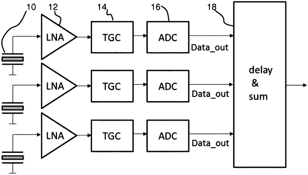
a plurality of ultrasound transducer elements arranged in an array, wherein the ultrasound transducer elements are configured to emit ultrasound pulses, receive reflected ultrasound pulses, and output corresponding signals; and
a plurality of signal processing circuits associated with the plurality of ultrasound transducer elements, respectively, wherein each signal processing circuit comprises:
an amplifier configured to amplify a signal received from an ultrasound transducer element of the plurality of ultrasound transducer elements and to output an amplified signal;
a switch arrangement at an output of the amplifier, wherein the switch arrangement is configured to receive the amplified signal from the amplifier and to generate an intermediate two-terminal output, by selectively outputting the amplified signal directly or with inversion;
a time gain compensation circuit configured to perform time gain compensation of the intermediate two-terminal output;
an analog to digital converter (ADC) at an output of the time gain compensation circuit, wherein the ADC is configured to digitize the intermediate two-terminal output to provide a digital signal; and
an inverter at an output of the ADC, wherein the inverter is configured to selectively invert the digital signal, synchronously with the switch arrangement outputting the amplified signal with inversion.
|