US 11,719,748 B2
Method of testing memory device employing limited number of test pins and memory device utilizing same
Xiaodong Xu, Wuhan (CN); Xiangming Zhao, Wuhan (CN); Shunlin Liu, Wuhan (CN); and Yi Chen, Wuhan (CN)
Assigned to YANGTZE MEMORY TECHNOLOGIES CO., LTD., Wuhan (CN)
Filed by YANGTZE MEMORY TECHNOLOGIES CO., LTD., Wuhan (CN)
Filed on Aug. 10, 2021, as Appl. No. 17/399,033.
Application 17/399,033 is a continuation of application No. 16/726,098, filed on Dec. 23, 2019, granted, now 11,125,816.
Application 16/726,098 is a continuation of application No. PCT/CN2019/111614, filed on Oct. 17, 2019.
Prior Publication US 2021/0364570 A1, Nov. 25, 2021
This patent is subject to a terminal disclaimer.
Int. Cl. G01R 31/28 (2006.01); G01R 31/317 (2006.01); G01R 31/3185 (2006.01); G11C 7/22 (2006.01); G11C 29/02 (2006.01)
CPC G01R 31/31713 (2013.01) [G01R 31/318572 (2013.01); G11C 7/222 (2013.01); G11C 29/023 (2013.01)] 20 Claims
OG exemplary drawing
 
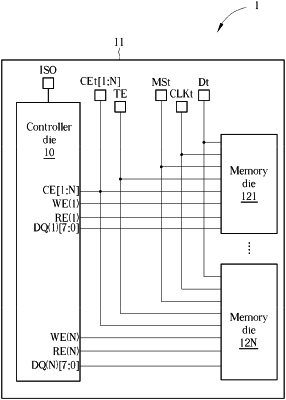
1. A memory device comprising:
a plurality of pins, comprising:
an isolation pin;
a test mode select pin configured to switch an operation mode of a memory die;
a test clock pin configured to receive a test clock; and
a test data pin configured to perform a data transmission;
a controller die coupled to the isolation pin, wherein the isolation pin is configured to provide an isolation control signal to indicate whether the memory die is to be isolated from the controller die; and
the memory die coupled to the test mode select pin, the test clock pin, and the test data pin.