| CPC G01R 31/2884 (2013.01) [H01L 23/66 (2013.01); H01L 2223/6611 (2013.01); H01L 2223/6616 (2013.01); H01L 2223/6677 (2013.01)] | 1 Claim |
|
1. A method of operating a semiconductor device including:
a substrate,
a circuit element disposed on a first surface side of the substrate,
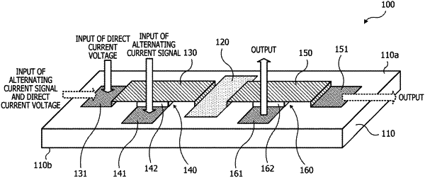
a first terminal that is disposed over the first surface side of the substrate and into which a first direct current voltage and a first alternating current signal for examination or a second direct current voltage for operation are input,
a first transmission line that has a first end coupled to the circuit element and a second end coupled to the first terminal and is disposed on the first surface side of the substrate in such a manner that the first transmission line is continuously in contact with the substrate between the first terminal and the circuit element,
a first dielectric that is disposed in a part of the first transmission line on a side opposite to the substrate in such a manner that the first dielectric is in contact with the first transmission line,
a second terminal that is disposed on a side of the first dielectric opposite to the first transmission line so as not to protrude from the first transmission line in a plan view and into which a second alternating current signal for operation is input,
a third terminal that is disposed on the first surface side of the substrate and from which a first output signal of the circuit element at a time of input of the first direct current voltage and the first alternating current signal into the first terminal is output,
a second transmission line that has a third end coupled to the circuit element and a fourth end coupled to the third terminal and is disposed on the first surface side of the substrate in such a manner that the first transmission line is continuously in contact with the substrate between the third terminal and the circuit element,
a second dielectric that is disposed in a part of the second transmission line on a side opposite to the substrate in such a manner that the second dielectric is in contact with the second transmission line,
a fourth terminal that is disposed on a side of the second dielectric opposite to the second transmission line so as not to protrude from the second transmission line in a plan view and from which a second output signal of the circuit element at a time of input of the second direct current voltage into the first terminal and input of the second alternating current signal into the second terminal is output, and
a conductor that is disposed on a second surface side of the substrate opposite to the first surface and set to a ground electric potential,
the method comprising:
inputting the first direct current voltage and the first alternating current signal into the first terminal and acquiring the first output signal of the circuit element from the third terminal at a time of examination of the semiconductor device; and
inputting the second direct current voltage into the first terminal, inputting the second alternating current signal into the second terminal, and acquiring the second output signal of the circuit element from the fourth terminal at a time of operation after the examination.
|