| CPC G01R 31/2642 (2013.01) [G01N 21/1717 (2013.01); G01R 31/31721 (2013.01); G01R 31/40 (2013.01); G01R 31/42 (2013.01); G01N 2021/1719 (2013.01); H02S 50/00 (2013.01); H02S 50/10 (2014.12); H02S 99/00 (2013.01)] | 9 Claims |
|
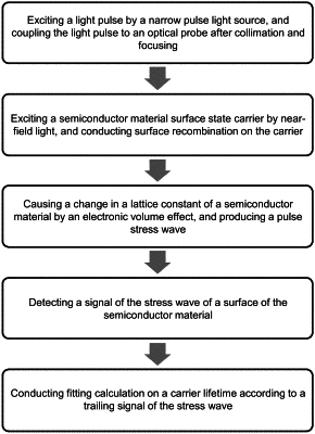
1. A method for testing a lifetime of a surface state carrier of a semiconductor, comprising the following steps:
1) Using a narrow pulse light source with photon energy higher than a semiconductor forbidden band width to emit a light pulse, coupling the light pulse to an interior of a near-field optical probe through light path collimation, and producing, by the near-field optical probe, a photon-generated carrier on a surface of a semiconductor material under test through excitation;
2) Concentrating the excited photon-generated carrier on the surface of the semiconductor material, and conducting recombination continuously with a surface state as a recombination center, wherein a recombination rate is in direct proportion to a carrier concentration and a carrier lifetime;
3) In both carrier excitation and recombination processes in step 1) and step 2), producing a change in a lattice constant due to an electronic volume effect, producing a stress wave, and detecting a signal of the stress wave in a high-frequency broadband ultrasonic testing mode; and
4) Conducting fitting calculation on the signal of the stress wave to obtain the lifetime of the surface state carrier τc.
|