| CPC G01N 27/27 (2013.01) [G01N 21/658 (2013.01); H01L 29/413 (2013.01); H01J 37/26 (2013.01)] | 11 Claims |
|
1. A method of manufacturing a multimodal sensor using a three-dimensional nanostructure, the method comprising:
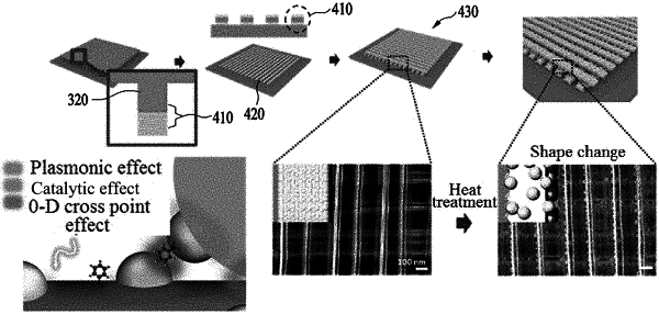
forming multi-layered nanowires including a multifunctional material;
transferring the multi-layered nanowires, each including both a first functional material and a second functional material, simultaneously to form a plurality of layers, each layer comprising a single multi-layered nanowire conforming to one of a plurality of base patterns, on a target substrate to form the three-dimensional nanostructure;
heat-treating the three-dimensional nanostructure; and
forming electrode layers including a first electrode pattern and a second electrode pattern which are formed on both sides of the heat-treated three-dimensional nanostructure, respectively, to form the multimodal sensor,
wherein each of the multi-layered nanowires is formed by sequentially depositing the second functional material, the first functional material, and the second functional material on each of said base patterns, which are formed on a base substrate;
wherein forming the nanowires includes:
applying a material on a master substrate where a plurality of master patterns is formed, wherein the material is sufficiently soft to be molded by the plurality of master patterns;
separating the material from the master substrate using an adhesive film and forming the base substrate, which includes the base patterns each having a reverse shape of each of the master patterns;
depositing the first functional material on the base patterns; and
depositing the second functional material having properties different from the first functional material on the first functional material to form the nanowires; and
wherein the first electrode pattern and the second electrode pattern are electrically insulated from each other and are formed in an interdigitated type.
|