| CPC G01N 23/20008 (2013.01) [G01N 23/201 (2013.01); G03F 7/70633 (2013.01); H01J 3/022 (2013.01); H01J 35/065 (2013.01); H01J 35/066 (2019.05); H01J 35/147 (2019.05); H01J 35/18 (2013.01); H05G 1/02 (2013.01); G01N 2223/03 (2013.01); G01N 2223/054 (2013.01); G01N 2223/1016 (2013.01); G01N 2223/204 (2013.01); G01N 2223/6116 (2013.01); H01J 2235/062 (2013.01); H01J 2235/068 (2013.01); H01J 2235/16 (2013.01); H01J 2235/18 (2013.01)] | 34 Claims |
|
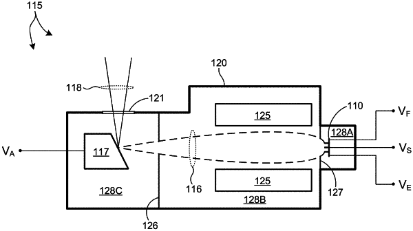
1. An x-ray illumination source, comprising:
an electron emitter array including a plurality of electron emitters each fabricated on a common substrate, each of the plurality of electron emitters comprising:
an emitter structure fabricated on the common substrate, the emitter structure extending from a surface plane of the common substrate in a direction normal to the surface plane, the emitter structure terminating at a sharp tip of the emitter structure;
an extractor electrode fabricated around the sharp tip of the emitter structure, wherein a void separates the emitter tip and at least a portion of the extractor electrode; and
a first insulating layer disposed between the emitter structure and the extractor electrode, wherein the first insulating layer electrically isolates the emitter structure from the extractor electrode, wherein a difference in electrical potential between the emitter structure and the extractor electrode stimulates an electron current flow from the sharp tip of the emitter structure;
an anode structure spatially separated from the electron emitter array, wherein a difference in electrical potential between the anode structure and the substrate accelerates the electron current flow from each of the plurality of electron emitters of the electron emitter array to the anode, wherein the incidence of the electron current flow onto the anode structure stimulates X-ray emission from the anode structure;
an electron lens located around a path of the electron current flow from the electron emitter array to the anode structure;
a first barrier separating a first portion of a vacuum chamber and a second portion of the vacuum chamber, wherein the electron emitter array is disposed in the first portion of the vacuum chamber and the electron lens is disposed in the second portion of the vacuum chamber, and wherein the first portion of the vacuum chamber is maintained at a lower pressure than the second portion of the vacuum chamber; and
a second barrier separating a third portion of the vacuum chamber and the second portion of the vacuum chamber, wherein the anode structure is disposed in the third portion of the vacuum chamber, wherein the second portion of the vacuum chamber is maintained at a lower pressure than the third portion of the vacuum chamber.
|