| CPC G01N 21/6428 (2013.01) [C12Q 1/6869 (2013.01); G01N 21/645 (2013.01); G01N 21/6408 (2013.01); G01N 21/6458 (2013.01); G01S 7/4865 (2013.01); H01L 27/14603 (2013.01); H01L 27/14687 (2013.01); H01L 27/14812 (2013.01); G01N 2021/6439 (2013.01); G01N 2021/6441 (2013.01); G01N 2201/0697 (2013.01); G01N 2201/06113 (2013.01); G01S 7/4863 (2013.01)] | 7 Claims |
|
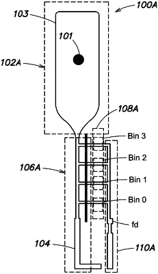
1. An integrated circuit, comprising:
a photodetection region configured to receive incident photons, the photodetection region being configured to produce a plurality of charge carriers in response to the incident photons;
at least one charge carrier storage region; and
a charge carrier segregation structure configured to selectively direct charge carriers of the plurality of charge carriers into the at least one charge carrier storage region based upon times at which the plurality of charge carriers are produced,
wherein the integrated circuit further comprises a semiconductor material with a graded doping concentration to establish a lateral electric field for driving the plurality of charge carriers toward the at least one charge carrier storage region,
wherein the charge carrier segregation structure is configured to aggregate, in the at least one charge carrier storage region, charge carriers of the plurality of charge carriers produced in response to a plurality of respective excitation light pulses.
|