| CPC G01N 21/6428 (2013.01) [C12Q 1/6869 (2013.01); G01N 21/64 (2013.01); G01N 21/6408 (2013.01); G01S 7/4865 (2013.01); H01L 27/14603 (2013.01); H01L 27/14612 (2013.01); H01L 27/14643 (2013.01); H01L 27/14687 (2013.01); H01L 27/14689 (2013.01); H01L 27/14812 (2013.01); H04N 25/77 (2023.01); G01N 21/6458 (2013.01)] | 24 Claims |
|
1. An integrated circuit, comprising:
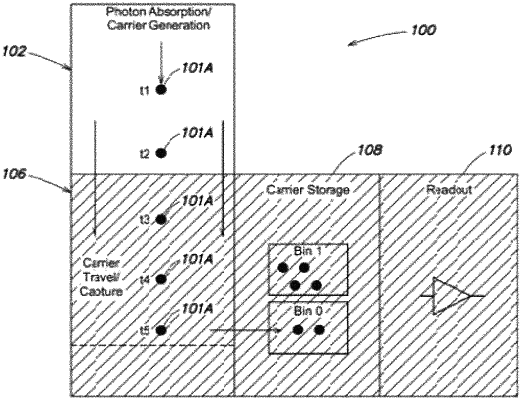
a photodetection region configured to receive incident photons, the photodetection region being configured to produce a plurality of charge carriers in response to the incident photons;
at least one charge carrier storage region;
a charge carrier segregation structure configured to selectively direct charge carriers of the plurality of charge carriers into the at least one charge carrier storage region based upon times at which the plurality of charge carriers are produced, wherein the charge carrier segregation structure is configured to transfer the plurality of charge carriers into the at least one charge carrier storage region without capturing the plurality of charge carriers between the photodetection region and the at least one charge carrier storage region, wherein the charge carrier segregation structure is configured to aggregate, in the at least one charge carrier storage region, first charge carriers produced in response to first photons of the incident photons, the first photons being produced by at least one luminescent molecule in response to excitation light pulses; and
a charge carrier rejection region configured to receive, during a rejection period, second charge carriers produced in the photodetection region in response to second photons of the incident photons, the excitation light pulses comprising the second photons.
|