US 11,719,634 B2
Highly stable semiconductor lasers and sensors for III-V and silicon photonic integrated circuits
Jerry R. Meyer, Catonsville, MD (US); Igor Vurgaftman, Severna Park, MD (US); Chadwick Lawrence Canedy, Washington, DC (US); William W. Bewley, Falls Church, VA (US); Chul Soo Kim, Springfield, VA (US); Charles D. Merritt, Fairfax, VA (US); Michael V. Warren, Arlington, VA (US); R. Joseph Weiblen, Washington, DC (US); and Mijin Kim, Springfield, VA (US)
Assigned to The Government of the United States of America, as represented by the Secretary of the Navy, Arlington, VA (US)
Filed by The Government of the United States of America, as represented by the Secretary of the Navy, Arlington, VA (US)
Filed on Aug. 20, 2021, as Appl. No. 17/407,274.
Application 17/407,274 is a continuation of application No. 16/509,613, filed on Jul. 12, 2019, granted, now 11,125,689.
Claims priority of provisional application 62/697,419, filed on Jul. 13, 2018.
Prior Publication US 2021/0396670 A1, Dec. 23, 2021
This patent is subject to a terminal disclaimer.
Int. Cl. G01N 21/59 (2006.01); H01S 5/028 (2006.01); H01S 5/10 (2021.01); H01S 5/125 (2006.01); H01S 5/34 (2006.01); H01S 5/343 (2006.01); H01S 5/042 (2006.01); H01S 5/20 (2006.01); H01S 5/02 (2006.01); H01S 5/026 (2006.01); G02B 6/10 (2006.01); G01N 21/27 (2006.01); G01N 21/25 (2006.01); G01J 3/18 (2006.01); G01J 3/28 (2006.01); H01S 5/22 (2006.01); H01S 5/06 (2006.01); H01S 5/062 (2006.01)
CPC G01N 21/59 (2013.01) [G01J 3/1895 (2013.01); G01J 3/2803 (2013.01); G01N 21/255 (2013.01); G01N 21/27 (2013.01); G02B 6/102 (2013.01); H01S 5/0215 (2013.01); H01S 5/0262 (2013.01); H01S 5/0287 (2013.01); H01S 5/0421 (2013.01); H01S 5/101 (2013.01); H01S 5/125 (2013.01); H01S 5/2063 (2013.01); H01S 5/2206 (2013.01); H01S 5/3402 (2013.01); H01S 5/343 (2013.01); G01N 2201/0612 (2013.01); H01S 5/062 (2013.01); H01S 5/0612 (2013.01)] 2 Claims
OG exemplary drawing
 
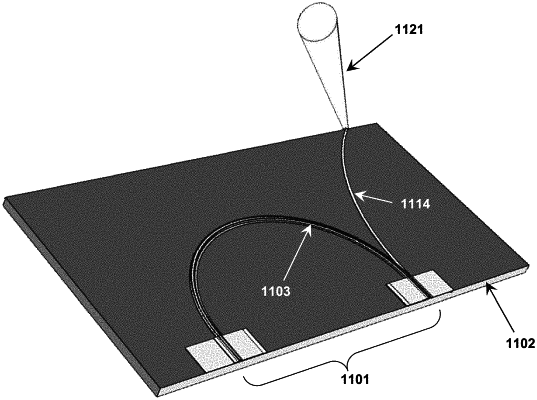
1. A highly stable semiconductor laser, comprising: a laser cavity comprising a first end and a second end, the first end terminating at a highly-reflective facet coated with a dielectric spacer and a highly reflective metal, and the second end terminating at a different position on the same facet that is coated with the same dielectric spacer and the same highly reflective metal, the laser cavity further comprising an active narrow-ridge waveguide situated within the laser cavity; wherein the highly reflective metal coating the facet prevents laser light produced in the active narrow-ridge waveguide from being passed from the first and second ends of the laser cavity and being fed back into the laser cavity following interactions of the laser light with external optical elements; wherein curving portions of the laser cavity allow both ends to terminate at different positions on the same highly-reflective facet; the laser further including a passive waveguide situated within the laser cavity and that runs parallel to a predefined portion of the active narrow-ridge waveguide; wherein a predetermined fraction of light from the active narrow-ridge waveguide is tunably passed to the passive waveguide via evanescent coupling, the evanescent coupling to the passive waveguide providing a single pathway for coupling light into or out of the laser cavity to an optical element outside the laser cavity; and wherein an extent of the evanescent coupling between the active narrow-ridge waveguide and the passive waveguide and corresponding output from the laser cavity is tuned by tuning a distance between the active narrow-ridge waveguide and passive waveguide or by tuning a length of the laser cavity over which the active narrow-ridge waveguide and passive waveguide run in parallel.