| CPC C23C 16/45538 (2013.01) [C23C 16/045 (2013.01); C23C 16/402 (2013.01); H01L 21/0228 (2013.01); H01L 21/02164 (2013.01)] | 5 Claims |
|
1. A deposition method comprising:
performing a plurality of atomic layer deposition cycles each including:
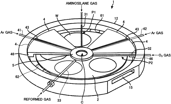
causing aminosilane gas to be adsorbed on a substrate in which a recessed portion is formed on a surface of the substrate;
causing a silicon oxide film to be stacked on the substrate by supplying oxidation gas to the substrate to oxidize the aminosilane gas adsorbed on the substrate; and
performing a reforming process on the silicon oxide film by exposing the silicon oxide film to a plasma formed from a reform gas including an oxygen gas and a first gas; and
changing the first gas from an argon gas to a helium gas during the performing of the atomic layer deposition cycles, wherein the first gas is the argon gas during a former part of the atomic layer deposition cycles, and is the helium gas during a latter part of the atomic layer deposition cycles,
wherein the first atomic layer deposition cycle is performed using the oxygen gas and the argon gas.
|