| CPC A61B 5/0285 (2013.01) [A61B 5/0059 (2013.01); A61B 5/0261 (2013.01); A61B 5/02141 (2013.01); A61B 5/7203 (2013.01); G01P 5/26 (2013.01); A61B 2562/0233 (2013.01); A61B 2562/182 (2013.01)] | 14 Claims |
|
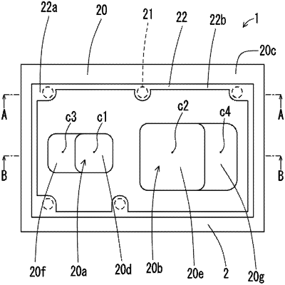
1. A measurement sensor package, comprising:
a substrate including a plurality of dielectric layers stacked on one another, the substrate being a rectangular plate and including a first recess and a second recess formed within a first surface thereof, the first recess being configured to contain a light emitter, the second recess being configured to contain a light receiver, the second recess being different and separate from the first recess,
the first recess including a first bottom surface on which the light emitter is mountable, and an inner side surface having a first step with a first step surface extending in a plane direction of the first surface,
the first step surface having a first connection pad thereon, the first connection pad being electrically connectable to the light emitter,
the second recess including a second bottom surface on which the light receiver is mountable, and an inner side surface having a second step with a second step surface extending in the plane direction of the first surface,
the second step surface having a second connection pad thereon, the second connection pad being electrically connectable to the light receiver,
wherein in a direction connecting a center of the first bottom surface and a center of the second bottom surface in a plan view, the first step surface is located outward from the first bottom surface and the second step surface is located outward from the second bottom surface,
the first step surface is located between the first bottom surface and the first surface in a vertical direction, and the second step surface is located between the second bottom surface and an internal portion of the first surface in the vertical direction,
a first signal via conductor connecting from the first connection pad on the first step surface to an external connection terminal through the substrate, and
a second signal via conductor connecting from the second connection pad on the second step surface to the external connection terminal through the substrate.
|