US 11,716,891 B2
Organic light emitting display module and organic light emitting display device having the same
Yong-hwan Park, Cheonan-si (KR); Jongseok Kim, Yongin-si (KR); Miyoung Kim, Daegu (KR); and Chiwook An, Hwaseong-si (KR)
Assigned to Samsung Display Co., Ltd., Yongin-Si (KR)
Filed by Samsung Display Co., Ltd., Yongin-Si (KR)
Filed on Nov. 4, 2022, as Appl. No. 17/980,604.
Application 17/980,604 is a continuation of application No. 17/327,846, filed on May 24, 2021, granted, now 11,522,020.
Application 17/327,846 is a continuation of application No. 16/870,832, filed on May 8, 2020, granted, now 11,018,205, issued on May 25, 2021.
Application 16/870,832 is a continuation of application No. 16/562,479, filed on Sep. 6, 2019, granted, now 10,651,246, issued on May 12, 2020.
Application 16/562,479 is a continuation of application No. 15/667,429, filed on Aug. 2, 2017, granted, now 10,418,425, issued on Sep. 17, 2019.
Claims priority of application No. 10-2016-0098607 (KR), filed on Aug. 2, 2016.
Prior Publication US 2023/0059081 A1, Feb. 23, 2023
Int. Cl. H10K 59/40 (2023.01); G06F 1/16 (2006.01); G06F 3/044 (2006.01); H10K 59/88 (2023.01); H10K 59/131 (2023.01); H10K 77/10 (2023.01); G06F 3/041 (2006.01); H10K 102/00 (2023.01)
CPC H10K 59/40 (2023.02) [G06F 1/1643 (2013.01); G06F 1/1652 (2013.01); G06F 3/0412 (2013.01); G06F 3/0443 (2019.05); G06F 3/0446 (2019.05); H10K 59/131 (2023.02); H10K 59/88 (2023.02); H10K 77/111 (2023.02); G06F 2203/04102 (2013.01); G06F 2203/04103 (2013.01); G06F 2203/04111 (2013.01); G06F 2203/04112 (2013.01); H10K 2102/311 (2023.02); Y02E 10/549 (2013.01)] 13 Claims
OG exemplary drawing
 
1. A display device comprising:
a base layer including a display area and a non-display area;
a display element layer comprising a display element on the display area;
a touch sensing member disposed on the display element layer and comprising a touch pattern on the display area;
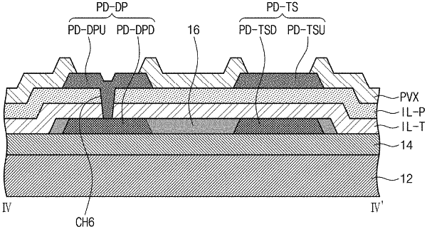
a first pad disposed in the non-display area;
a second pad disposed on the first pad;
an organic layer disposed between the base layer and the second pad, and the organic layer partially covering the first pad; and
an inorganic layer disposed between the organic layer and the second pad, and the inorganic layer exposing at least a portion of the first pad, and
wherein the second pad is electrically connected to one of the display element layer and the touch sensing member.