US 11,716,858 B1
Ferroelectric device film stacks with texturing layer which is part of a bottom electrode and a barrier, and method of forming such
Niloy Mukherjee, San Ramon, CA (US); Ramamoorthy Ramesh, Moraga, CA (US); Sasikanth Manipatruni, Portland, OR (US); James Clarkson, Berkeley, CA (US); Fnu Atiquzzaman, Orinda, CA (US); Gabriel Antonio Paulius Velarde, San Leandro, CA (US); and Jason Y. Wu, Albany, CA (US)
Assigned to Kepler Computing Inc., San Francisco, CA (US)
Filed by Kepler Computing Inc., San Francisco, CA (US)
Filed on May 7, 2021, as Appl. No. 17/315,143.
Application 17/315,143 is a continuation of application No. 17/315,111, filed on May 7, 2021.
This patent is subject to a terminal disclaimer.
Int. Cl. H10B 53/30 (2023.01); H01L 27/115 (2017.01); H01L 49/02 (2006.01)
CPC H10B 53/30 (2023.02) [H01L 28/75 (2013.01)] 19 Claims
OG exemplary drawing
 
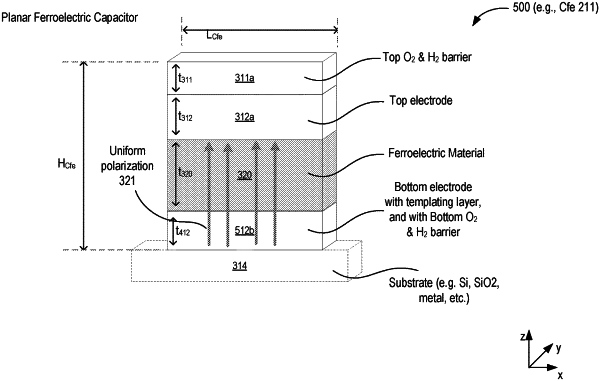
1. A ferroelectric device comprising:
a first structure comprising ferroelectric material;
a second structure over the first structure, the second structure comprising metallic electrode; and
a third structure under the first structure, wherein the third structure is self-crystallized and is a single layer, and wherein the third structure is to:
induce crystallographic orientation in the first structure;
provide conductive characteristics of an electrode; and
provide diffusion barrier from oxygen and hydrogen.