| CPC H10B 12/315 (2023.02) [H10B 12/34 (2023.02)] | 20 Claims |
|
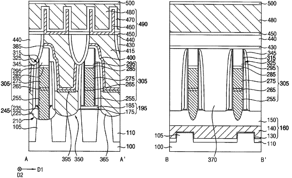
1. A semiconductor device comprising:
an active pattern on a substrate; a gate structure buried at an upper portion of the active pattern;
a bit line structure having a first conductive pattern, wherein a lowermost portion of the first conductive pattern is in direct contact with an upper surface of the active pattern;
a lower spacer structure covering a lower sidewall of the bit line structure;
a contact plug structure on the active pattern and adjacent to the bit line structure; and a capacitor on the contact plug structure,
wherein,
the lower spacer structure includes a first lower spacer and a second lower spacer that are sequentially stacked from the lower sidewall of the bit line structure in a horizontal direction that is parallel to an upper surface of the substrate,
the first lower spacer includes an oxide, and contacts the lower sidewall of the bit line structure, but does not contact the contact plug structure, and
the second lower spacer includes a material different from any of the materials of the first lower spacer.
|