| CPC H05K 7/1489 (2013.01) [H01P 3/16 (2013.01); H01P 5/12 (2013.01); H05K 1/0243 (2013.01); H01L 23/5384 (2013.01); H01L 23/5386 (2013.01); H01L 23/66 (2013.01); H01L 24/16 (2013.01); H01L 25/18 (2013.01); H01L 2223/6616 (2013.01); H01L 2223/6627 (2013.01); H01L 2224/16225 (2013.01); H05K 1/181 (2013.01); H05K 2201/10356 (2013.01); H05K 2201/10378 (2013.01); H05K 2201/10734 (2013.01)] | 19 Claims |
|
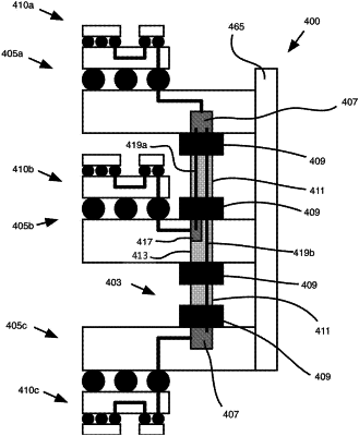
9. A computing device comprising:
a first printed circuit board (PCB) physically coupled with a chassis at a first vertical location, wherein the first PCB includes a first microelectronic package electrically coupled to the first PCB and a first waveguide communicatively coupled with the first microelectronic package;
a second PCB physically coupled with the chassis at a second vertical location below the first PCB, wherein the second PCB includes a second microelectronic package electrically coupled to the second PCB and a second waveguide communicatively coupled with the second microelectronic package;
a third PCB physically coupled with the chassis at a third vertical location below the second PCB such that the second PCB is physically located between the first PCB and the third PCB, wherein the third PCB includes a third microelectronic package electrically coupled to the third PCB and a third waveguide communicatively coupled with the third microelectronic package; and
a fourth waveguide communicatively coupled with the first waveguide on the first PCB, the second waveguide on the second PCB, and the third waveguide on the third PCB, wherein at least a portion of the fourth waveguide is oriented vertically, and wherein the first, second, third, and fourth waveguides communicatively couple the first microelectronic package, the second microelectronic package, and the third microelectronic package to each other.
|