| CPC H05K 3/424 (2013.01) [C25D 7/00 (2013.01); H05K 3/0023 (2013.01); H05K 3/0044 (2013.01); H05K 3/425 (2013.01); H05K 2203/0723 (2013.01)] | 13 Claims |
|
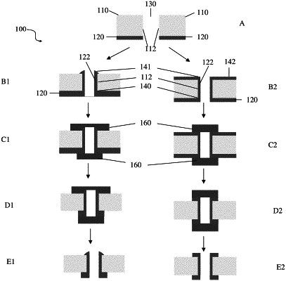
1. A method of creating an electrically conductive via in a substrate having a first side and a second side, comprising the ordered steps of:
creating a channel through the substrate; and
using electrolytic plating to deposit a metal procedurally on the substrate, first from a conductor at a first region about the channel on the first side of the substrate, then along a wall of the channel, and then to a second region about the second side of the substrate;
further comprising placing a plating resist onto a portion of the substrate, thereby further protecting the substrate from metal deposition, wherein the plating resist only inhibits metal deposition by electroless plating, and is a polymer.
|