| CPC H03K 3/012 (2013.01) [H03K 5/02 (2013.01)] | 12 Claims |
|
1. A chip with pad tracking, comprising:
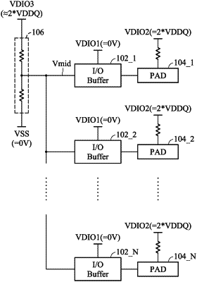
a first input/output buffer and a first pad, wherein the first input/output buffer powered by a first power is coupled to the first pad, and the first pad is coupled to a system power;
a second input/output buffer and a second pad, wherein the second input/output buffer powered by the first power is coupled to the second pad, and the second pad is coupled to the system power; and
a bias circuit, generating a bias signal which is dispatched to the first input/output buffer and the second input/output buffer to block a first leakage path within the first input/output buffer and a second leakage path within the second input/output buffer when the system power is on and the first power is off;
wherein:
the first input/output buffer comprises a first floating N-well pull-up string, and a first pad-tracking circuit;
according to the bias signal, the first pad-tracking circuit couples the first pad to a gate and a bulk of a first leakage-blocking transistor of the first floating N-well pull-up string;
the second input/output buffer comprises a second floating N-well pull-up string, and a second pad-tracking circuit; and
according to the bias signal, the second pad-tracking circuit couples the second pad to a gate and a bulk of a second leakage-blocking transistor of the second floating N-well pull-up string.
|