| CPC H01S 5/0234 (2021.01) [G02F 1/015 (2013.01); H01S 5/0237 (2021.01); H01S 5/02234 (2021.01); H01S 5/02325 (2021.01); H01S 5/0261 (2013.01)] | 20 Claims |
|
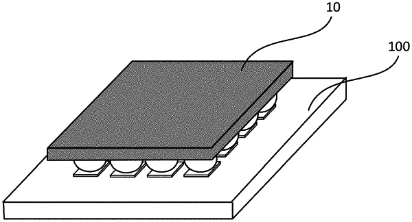
1. An integrated circuit (IC) assembly comprising:
a support;
a semiconductor die including a device, the semiconductor die mounted to the support with the device facing the support;
a first layer comprising decoupling material on the device, the decoupling material in direct contact with the device; and
a second layer comprising an underfill material between the semiconductor die and the support, wherein the decoupling material is between the device and the underfill material and has a chemical composition that precludes covalent and ionic bonds with the underfill material.
|