| CPC H01Q 21/24 (2013.01) [H05K 1/0243 (2013.01); H05K 1/0248 (2013.01); H01P 9/00 (2013.01); H05K 2201/10098 (2013.01)] | 30 Claims |
|
1. A printed circuit board comprising:
a first layer and a second layer substantially parallel to and spaced apart from the first layer;
an integrated circuit connected to the first layer and configured to provide a first electronic signal over a first conductive path between a first pair of conductive points and a second electronic signal over a second conductive path between a second pair of conductive points;
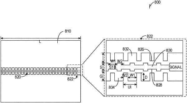
wherein the first conductive path includes a first narrow section extending between a first broad section and a second broad section, wherein:
the first narrow section has a first dimension; and
the first broad section and the second broad section have a second dimension, the second dimension greater than the first dimension; and
wherein the second conductive path includes a finger extending toward the narrow section of the first conductive path and having a third dimension, the third dimension greater than the second dimension.
|