| CPC H01L 29/6681 (2013.01) [H01L 21/266 (2013.01); H01L 21/26506 (2013.01); H01L 21/30604 (2013.01); H01L 29/0653 (2013.01); H01L 29/0673 (2013.01); H01L 29/42392 (2013.01); H01L 29/6653 (2013.01); H01L 29/66545 (2013.01); H01L 29/66553 (2013.01); H01L 29/7853 (2013.01)] | 20 Claims |
|
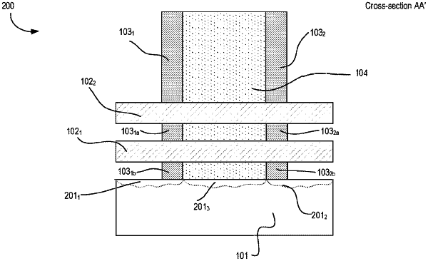
1. An integrated circuit comprising:
a nanowire or nanoribbon having an upper surface and a lower surface, the upper and lower surfaces of the nanowire or nanoribbon extending in a lateral direction;
an individual pair of spacers of one or more pairs of spacers, the individual pair of spacers comprising a first spacer adjacent to a first side of the nanowire or nanoribbon and a second spacer adjacent to a second side of the nanowire or nanoribbon; and
a layer of crystalline silicon below the nanowire or nanoribbon, the layer having one or more upper portions and a lower portion, the one or more upper portions of the layer each having a surface extending in the lateral direction, wherein the one or more upper portions of the layer comprises a first silicon crystal structure, and the lower portion of the layer comprises a second silicon crystal structure distinct from the first silicon crystal structure.
|