| CPC H01L 29/4991 (2013.01) [H01L 21/28088 (2013.01); H01L 21/28123 (2013.01); H01L 21/764 (2013.01); H01L 29/4966 (2013.01); H01L 29/516 (2013.01); H01L 29/6653 (2013.01); H01L 29/6656 (2013.01); H01L 29/6684 (2013.01); H01L 29/66545 (2013.01); H01L 29/78391 (2014.09)] | 19 Claims |
|
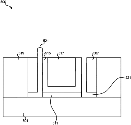
1. A method of forming an airgap in a semiconductor structure, the method comprising:
forming a high-k material on a floor of a trench, wherein the trench is defined on a semiconductor substrate between sidewalls of a first material and a spacer material;
forming a gate structure on the high-k material wherein the gate structure contacts the first material along each sidewall of the trench;
forming a source/drain material next to the spacer material; and
etching the first material, wherein the etching forms an airgap adjacent the gate structure and underneath the spacer material from the high-k material to a sidewall of the source/drain material.
|