| CPC H01L 29/36 (2013.01) [H01L 21/265 (2013.01); H01L 29/0615 (2013.01); H01L 29/1095 (2013.01)] | 16 Claims |
|
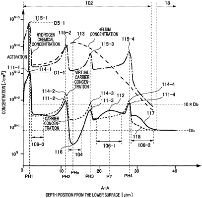
1. A semiconductor device comprising a semiconductor substrate, comprising:
a hydrogen containing region including hydrogen;
a high concentration region in the hydrogen containing region, the high concentration region having a higher carrier concentration than a virtual carrier concentration determined based on a concentration of the hydrogen included and an activation ratio of the hydrogen, wherein
a carrier concentration distribution in a depth direction of the hydrogen containing region has a plurality of first peaks,
the high concentration region is arranged between two adjacent ones of the plurality of first peaks in the depth direction,
a carrier concentration distribution of the high concentration region has a second peak in the depth direction, and
the second peak in the high concentration region has a full width at half maximum greater than a full width at half maximum of any of the plurality of first peaks.
|