| CPC H01L 29/157 (2013.01) [H01L 29/0619 (2013.01); H01L 29/205 (2013.01); H01L 29/861 (2013.01)] | 18 Claims |
|
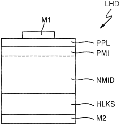
1. A stacked high barrier III-V power semiconductor diode comprising:
at least a regionally formed first metallic terminal contact layer;
a semiconductor contact region of a first conductivity type with a dopant concentration greater than 1×10¹⁸ N/cm3 and with a first lattice constant;
a drift layer of a second conductivity type with the first lattice constant and with a layer thickness greater than 10 microns;
a doped intermediate layer of the first conductivity type with a dopant concentration of less than 5×10¹⁸ N/cm3, with the first lattice constant and with a thickness between 1 micron and 30 microns;
a metamorphic buffer layer sequence of the second conductivity type with a layer thickness of more than 0.2 microns and less than 20 microns, the metamorphic buffer layer sequence having an upper side with the first lattice constant and a lower side with a second lattice constant, the upper side being arranged in a direction of the drift layer; and
a second metallic terminal contact layer formed below the lower side of the metamorphic buffer layer sequence,
wherein the first lattice constant is greater than the second lattice constant,
wherein the first metallic terminal contact layer, the semiconductor contact region, the drift layer, the intermediate layer, the metamorphic buffer layer sequence, the second metallic terminal contact layer are arranged in the order mentioned, and
wherein at least the semiconductor contact region and the drift layer and the metamorphic buffer layer sequence comprise a III-V compound.
|