| CPC H01L 27/14683 (2013.01) [H01L 25/18 (2013.01); H01L 27/14678 (2013.01)] | 20 Claims |
|
1. A method for integrating an image sensor and a light emitting diode (LED), comprising:
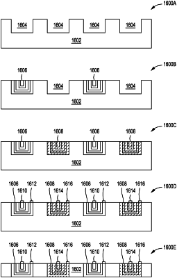
forming a plurality of cavities on a substrate, the plurality of cavities having at least one cavity profile and configured to accept an emitter pixel structure of the LED or a sensor pixel structure of the image sensor;
depositing or epitaxially growing, in situ, layer by layer, a first plurality of layers of at least one emitter pixel structure completely filling at least a first one of the plurality of cavities on the substrate, wherein the at least one emitter pixel structure is configured to have a plurality of exposed direct emitter contact areas on a same side and at a same height and wherein the exposed direct emitter contact areas are exposed areas of two or more different layers of the first plurality of layers; and
depositing or epitaxially growing, in situ, layer by layer, a second plurality of layers of at least one sensor pixel structure completely filling at least a second one of the plurality of cavities on the substrate adjacent to the at least one emitter pixel structure, wherein the at least one sensor pixel structure is configured to have a plurality of exposed direct sensor contact areas on a same side and at a same height and wherein the exposed direct sensor contact areas are exposed areas of two or more different layers of the second plurality of layers.
|