| CPC H01L 24/13 (2013.01) [H01L 23/49811 (2013.01); H01L 23/49822 (2013.01); H01L 24/14 (2013.01); H01L 24/16 (2013.01); H01L 24/81 (2013.01); H01L 25/18 (2013.01); H01L 2224/13019 (2013.01); H01L 2224/1403 (2013.01); H01L 2224/16227 (2013.01); H01L 2224/81345 (2013.01); H01L 2224/81815 (2013.01)] | 16 Claims |
|
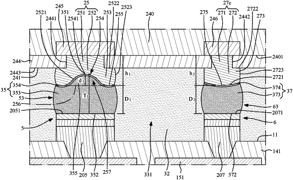
1. An electronic device, comprising:
a substrate;
a first bump disposed over the substrate, and having a first width, wherein an end portion of the first bump defines a first recess portion;
a second bump disposed over the substrate, and having a second width less than the first width; and
a first reflowable material disposed on the first bump and extending in the first recess portion,
wherein an elevation of a bottom of the first recess portion is different from an elevation of a bottom of a second recess portion.
|