| CPC H01L 24/08 (2013.01) [H01L 24/80 (2013.01); H01L 25/0657 (2013.01); H01L 25/18 (2013.01); H01L 25/50 (2013.01); H01L 2224/08145 (2013.01); H01L 2224/80895 (2013.01); H01L 2224/80896 (2013.01); H01L 2924/1431 (2013.01); H01L 2924/14511 (2013.01)] | 20 Claims |
|
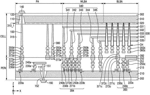
1. A nonvolatile memory device comprising:
a substrate including a first surface and a second surface opposite to the first surface in a first direction;
a common source line on the first surface of the substrate;
a plurality of word lines stacked on the common source line;
a first insulating pattern spaced apart from the plurality of word lines in a second direction crossing the first direction, and in the substrate;
an insulating layer on the second surface of the substrate;
a first contact plug penetrating the first insulating pattern and extending in the first direction;
a second contact plug penetrating the insulating layer, extending in the first direction, and connected to the first contact plug;
an upper bonding metal connected to the first contact plug and connected to a circuit element; and
a first input/output pad connected to the second contact plug and electrically connected to the circuit element.
|