| CPC H01L 24/08 (2013.01) [H01L 23/562 (2013.01); H01L 25/0657 (2013.01); H01L 25/18 (2013.01); H01L 2224/08145 (2013.01); H01L 2924/1431 (2013.01); H01L 2924/14511 (2013.01); H01L 2924/3511 (2013.01)] | 20 Claims |
|
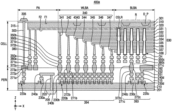
1. A nonvolatile memory device comprising:
an upper insulating layer;
a first substrate on the upper insulating layer;
an upper interlayer insulating layer on the first substrate;
a plurality of word lines stacked on the first substrate in a first direction and extending through a partial portion of the upper interlayer insulating layer;
a lower interlayer insulating layer on the upper interlayer insulating layer;
a second substrate on the lower interlayer insulating layer;
a lower insulating layer on the second substrate; and
a dummy pattern composed of dummy material, the dummy pattern is disposed in a trench formed in at least one of the first and second substrates, wherein the trench is formed on at least one of a surface where the upper insulating layer meets the first substrate, and a surface where the lower insulating layer meets the second substrate, the trench extending solely within the at least one of the first and second substrates.
|