| CPC H01L 23/5389 (2013.01) [H01L 21/486 (2013.01); H01L 21/4864 (2013.01); H01L 21/50 (2013.01); H01L 21/76802 (2013.01); H01L 23/13 (2013.01); H01L 23/147 (2013.01); H01L 23/49827 (2013.01); H01L 23/49838 (2013.01); H01L 23/49866 (2013.01); H01L 23/49894 (2013.01); H01L 23/5384 (2013.01); H01L 23/5385 (2013.01); H01L 23/5386 (2013.01); H01L 23/66 (2013.01); H01L 25/0657 (2013.01); H01L 25/105 (2013.01); H01L 27/0688 (2013.01); H01Q 1/2283 (2013.01); H01Q 1/243 (2013.01); H05K 1/0243 (2013.01); H01L 2021/60007 (2013.01); H01L 2225/107 (2013.01); H01L 2225/1035 (2013.01)] | 20 Claims |
|
1. A method of forming a stacked semiconductor device, comprising:
placing a first dielectric film over a semiconductor package, the semiconductor package comprising:
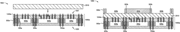
a first semiconductor die disposed within a first cavity of a first silicon substrate and embedded within a first insulating layer, the first insulating layer disposed over a first side and a second side of the first silicon substrate and contacting each side of the first semiconductor die; and
a first conductive interconnection disposed within a first via of the first silicon substrate and extending from at least the first side to the second side of the first silicon substrate, wherein the first insulating layer is disposed between the first conductive interconnection and a sidewall of the first via;
positioning a second silicon substrate over the first dielectric film, the second silicon substrate comprising a second cavity and a second via formed therein;
placing a second semiconductor die within the second cavity formed in the second silicon substrate;
laminating the first and second dielectric films to form a second insulating layer, the second insulating layer embedding the second semiconductor die within the second cavity; and
forming a second conductive interconnection within the second via.
|