| CPC H01L 23/5389 (2013.01) [H01L 21/4853 (2013.01); H01L 21/4857 (2013.01); H01L 21/561 (2013.01); H01L 21/565 (2013.01); H01L 21/568 (2013.01); H01L 21/6835 (2013.01); H01L 21/78 (2013.01); H01L 23/3128 (2013.01); H01L 23/5383 (2013.01); H01L 23/5386 (2013.01); H01L 24/19 (2013.01); H01L 24/20 (2013.01); H01L 2221/68372 (2013.01); H01L 2224/214 (2013.01)] | 20 Claims |
|
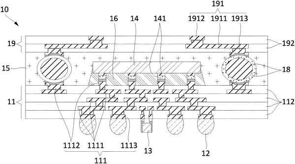
1. A semiconductor device, comprising:
a first redistribution layer (RDL) substrate comprising:
a first dielectric structure; and
a first conductive structure through the first dielectric structure and comprising one or more first conductive redistribution layers;
an electronic component over the first RDL substrate, wherein the electronic component is coupled with the first conductive structure;
a body over a top side of the first RDL substrate, wherein the electronic component is in the body;
a second RDL substrate comprising:
a second dielectric structure over the body; and
a second conductive structure through the second dielectric structure and comprising one or more second conductive redistribution layers; and
an internal interconnect coupled between the first conductive structure and the second conductive structure;
wherein:
the first conductive structure comprises a conductive path comprising a trace and a downward via extending downward from the trace, wherein the downward via and the trace comprise a same metallic layer;
the second conductive structure comprises a conductive path comprising a trace and an upward via extending upward from the trace, wherein the upward via and the trace comprise a same metallic layer; and
the body directly contacts the first RDL substrate and directly contacts the second RDL substrate.
|