| CPC H01L 23/5383 (2013.01) [H01L 21/486 (2013.01); H01L 21/4857 (2013.01); H01L 23/3128 (2013.01); H01L 23/5384 (2013.01)] | 12 Claims |
|
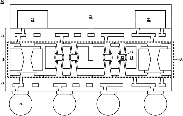
1. An embedded component package structure, comprising:
a magnetically permeable layer having a top surface;
a first conductive element in the magnetically permeable layer, wherein the first conductive element has a first substantially planar surface exposed from the magnetically permeable layer;
a conductive layer disposed on the top surface of the magnetically permeable layer and electrically connected with the first conductive element; and
a dielectric layer disposed between the conductive layer and the magnetically permeable layer, wherein the dielectric layer is in contact with a part of the first substantially planar surface of the first conductive element.
|