| CPC H01L 23/538 (2013.01) [G02B 6/30 (2013.01); H01L 23/66 (2013.01); H01P 3/16 (2013.01); H01P 11/006 (2013.01); H01L 2223/6627 (2013.01)] | 16 Claims |
|
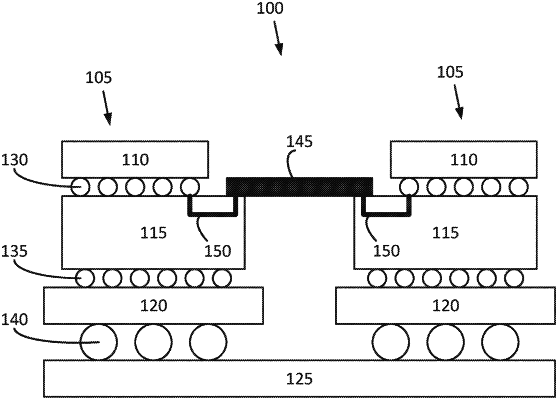
11. A method of forming a waveguide that is to be coupled with a package substrate of a semiconductor package, wherein the method comprises:
laminating a waveguide dielectric material on a sacrificial layer of a carrier;
developing the waveguide dielectric material into one or more waveguide channels; and
positioning an adhesive material on the waveguide dielectric material.
|