| CPC H01L 23/5223 (2013.01) [H01L 23/5226 (2013.01); H01L 23/5227 (2013.01); H01L 23/5228 (2013.01); H01L 24/20 (2013.01); H01L 24/24 (2013.01); H01L 25/0657 (2013.01); H01L 25/18 (2013.01); H01L 2224/2105 (2013.01); H01L 2224/24146 (2013.01); H01L 2924/1431 (2013.01); H01L 2924/14511 (2013.01); H10B 43/27 (2023.02)] | 18 Claims |
|
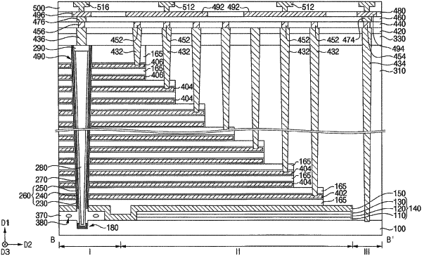
1. A semiconductor device, comprising:
a plurality of lower circuit patterns disposed on a lower substrate;
a plurality of lower bonding patterns disposed on the lower circuit patterns, the lower bonding patterns including a first conductive material and being electrically connected to the lower circuit patterns, respectively;
a plurality of upper bonding patterns disposed on and contacting the lower bonding patterns, respectively, the upper bonding patterns including a second conductive material;
a passive device disposed on the upper bonding patterns, the passive device including a third conductive material and contacting one of the upper bonding patterns;
a gate electrode structure disposed on the passive device, the gate electrode structure including gate electrodes spaced apart from each other in a first direction perpendicular to an upper surface of the lower substrate, each of the gate electrodes extending in a second direction parallel to the upper surface of the lower substrate,
wherein extension lengths of the gate electrodes increase from a lowermost level toward an uppermost level in a stepwise manner in the second direction;
a channel extending through at least a portion of the gate electrode structure;
an upper substrate disposed on the channel,
a first wiring disposed at a same level as the passive device, the first wiring being spaced apart from the passive device; and
a bit line extending between the first wiring and the channel in a third direction parallel to the upper surface of the lower substrate and crossing the second direction, the bit line being electrically connected to the channel and the first wiring,
wherein the passive device is electrically connected to neither the gate electrode structure nor the bit line.
|
|
12. A semiconductor device, comprising:
a plurality of lower circuit patterns disposed on a lower substrate, adjacent ones of the lower circuit patterns being spaced apart from each other by one of a plurality of isolation patterns;
a plurality of lower bonding patterns disposed on the lower circuit patterns, the lower bonding patterns including a first conductive material and being electrically connected to the lower circuit patterns, respectively;
a plurality of upper bonding patterns disposed on and contacting the lower bonding patterns, respectively, the upper bonding patterns including a second conductive material;
a first wiring disposed on the upper bonding patterns, the first wiring contacting ones of the upper bonding patterns;
a gate electrode structure disposed on the first wiring, the gate electrode structure including gate electrodes spaced apart from each other in a first direction perpendicular to an upper surface of the lower substrate, each of the gate electrodes extending in a second direction parallel to the upper surface of the lower substrate,
wherein extension lengths of the gate electrodes increase from a lowermost level toward an uppermost level in a stepwise manner in the second direction;
a channel extending through at least a portion of the gate electrode structure; and
an upper substrate disposed on the channel,
wherein ones of the lower circuit patterns are electrically connected with each other through the first wiring, the ones of the upper bonding patterns, and the lower bonding patterns contacting the ones of the upper bonding patterns, respectively.
|
|
16. A semiconductor device, comprising:
an upper substrate;
a plurality of memory cells disposed under the upper substrate;
a channel extending through at least a portion of the memory cells;
a passive device disposed under the memory cells;
a plurality of upper bonding patterns disposed under the passive device;
a plurality of lower bonding patterns disposed under and contacting the upper bonding patterns, respectively;
a plurality of transistors disposed under and electrically connected to the lower bonding patterns, respectively;
a lower substrate disposed under the transistors,
a first wiring disposed at a same level as the passive device, the first wiring being spaced apart from the passive device; and
a bit line extending between the first wiring and the channel, the bit line being electrically connected to the channel and the first wiring,
wherein the passive device is electrically connected to neither the memory cells nor the bit line,
wherein the passive device contacts one of the upper bonding patterns and is electrically connected to one of the transistors through the one of the upper bonding patterns.
|