| CPC H01L 23/49575 (2013.01) [H01L 21/4885 (2013.01); H01L 23/481 (2013.01); H01L 23/5383 (2013.01); H01L 23/5384 (2013.01); H01L 23/5387 (2013.01); H01L 23/5389 (2013.01); H01L 25/0657 (2013.01); H01L 25/072 (2013.01); H01L 25/165 (2013.01); H02M 3/156 (2013.01); H02M 1/0012 (2021.05)] | 18 Claims |
|
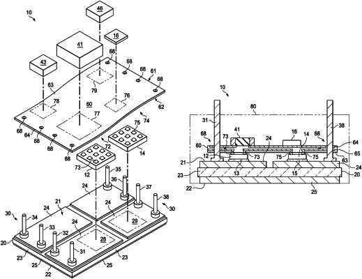
1. A semiconductor package comprising:
a substrate forming a first surface and a second surface that opposes the first surface;
a set of terminals protruding from the first surface of the substrate;
a power stage directly attached to the first surface of the substrate via an adhesive;
a substrate layer including at least one circuit layer forming power stage conductors and control circuit conductors, wherein the power stage is mounted on a first surface of the substrate layer such that the power stage is electrically connected to the power stage conductors,
wherein the power stage is between the substrate layer and the substrate; and
a die mounted on a second surface of the substrate layer opposite the power stage such that the die is electrically connected to the control circuit conductors,
wherein an output of the die is electrically connected to an input of the power stage via the control circuit conductors.
|