|
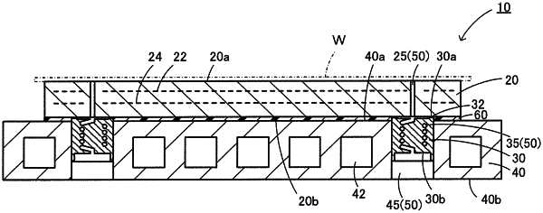
1. A member for a semiconductor manufacturing apparatus comprising: a ceramic plate having an upper surface serving as a wafer mounting surface and incorporating an electrode; a ceramic dense plug disposed adjacent to a lower surface side of the ceramic plate and ceramic-bonded to the ceramic plate by a ring-shaped joint portion; a metal cooling plate joined to the lower surface of the ceramic plate in a portion other than the joint portion; and a gas flow channel, wherein the gas flow channel includes a gas discharge hole that passes completely through the ceramic plate in a thickness direction of the ceramic plate and an internal gas flow channel that passes from an upper surface to a lower surface of the dense plug while winding through the dense plug, and wherein the gas flow channel passes inside of an inner periphery of the joint portion.
|