| CPC H01L 21/02057 (2013.01) [H01L 21/0254 (2013.01); H01L 21/02389 (2013.01); H01L 21/02433 (2013.01); H01L 21/3065 (2013.01); H01L 21/30612 (2013.01)] | 22 Claims |
|
1. A method for removing dry-etch damage from a substrate surface, the method comprising:
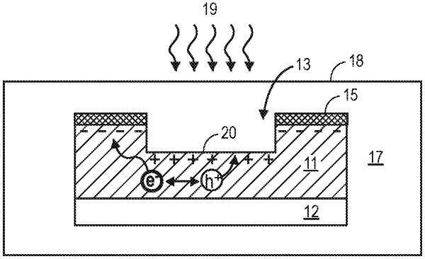
providing a substrate comprising an n-type Al/In/GaN semiconductor material;
dry-etching a surface of the substrate to form a dry etched surface comprising sidewalls and causing dry-etch damage to remain on the dry etched surface;
immersing the dry etched surface of the substrate in an electrolyte solution; and
illuminating the dry etched surface with above bandgap light having a wavelength that generates electron-hole pairs in the n-type Al/In/GaN semiconductor material, thereby photoelectrochemically (PEC) etching the dry etched surface to remove at least a portion of the dry-etch damage and form a PEC etched surface.
|