| CPC H01J 37/3244 (2013.01) [H01J 37/32183 (2013.01); H01J 37/32495 (2013.01); H01J 37/32522 (2013.01); H01J 37/32715 (2013.01); H01L 21/67069 (2013.01); H01J 2237/332 (2013.01); H01J 2237/334 (2013.01)] | 18 Claims |
|
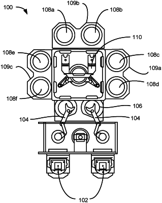
1. A semiconductor processing system comprising:
a pedestal configured to support a semiconductor substrate, the pedestal operable as a first plasma-generating electrode;
a lid plate defining a radial volume;
a faceplate supported with the lid plate, the faceplate operable as a second plasma-generating electrode, wherein a plasma processing region is defined between the pedestal and the faceplate within the radial volume defined by the lid plate, and wherein the faceplate defines a plurality of first apertures;
a showerhead positioned between the faceplate and the pedestal, wherein the showerhead defines a plurality of second apertures comprising a greater number of apertures than the plurality of first apertures;
an annular liner positioned within the radial volume defined by the lid plate, wherein the annular liner is characterized by a first surface facing the showerhead and a second surface opposite the first surface, wherein:
the annular liner defines a protrusion extending about an exterior surface of the annular liner; and
the protrusion is recessed from the first surface of the annular liner and defines a first ledge facing the first surface of the annular liner and a second ledge facing the second surface of the annular liner.
|