| CPC H01J 37/32027 (2013.01) [H01J 37/32045 (2013.01); H01J 37/32596 (2013.01)] | 20 Claims |
|
1. A method for processing a surface of a substrate, the method comprising:
processing the substrate via a direct-current (DC) plasma system, wherein the DC plasma system comprises:
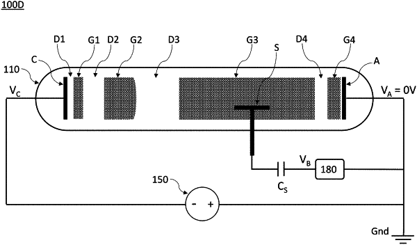
a DC plasma reaction chamber configured to contain a DC plasma that is generated between an anode and a cathode of the DC plasma reaction chamber;
an adjustable DC voltage source having an output that is electrically coupled to the anode;
a DC current source that is electrically coupled to the cathode; and
a substrate support stage arranged in a region of the DC plasma reaction chamber that contains a positive column of the DC plasma,
wherein
the adjustable DC voltage source and the DC current source are electrically coupled to a reference ground, and
the DC current source is configured to set, during the processing of the substrate, a constant DC current that flows between the anode and the cathode, and the adjustable DC voltage source is configured to adjust, during the processing of the substrate and independently from the constant DC current, an electrical potential at the anode to set a substrate floating potential at a surface of the substrate support stage to a potential of the reference ground.
|