| CPC H01J 1/3044 (2013.01) [H01J 3/022 (2013.01); H01J 37/073 (2013.01); H01J 35/065 (2013.01); H01J 37/28 (2013.01); H01J 37/3174 (2013.01)] | 20 Claims |
|
1. A light modulated electron source comprising:
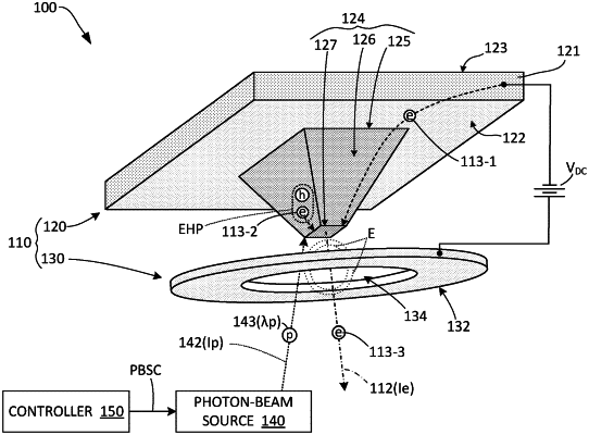
a field emitter cathode including a silicon substrate having opposing first and second surfaces, and an emitter protrusion having a base integrally connected to the silicon substrate, a body portion extending from the first surface, and an emission tip disposed at a distal end of the body portion;
a dielectric layer disposed on the first top surface adjacent to the emitter protrusion;
an extractor disposed on the dielectric layer and fixedly positioned adjacent to the field emitter cathode, the extractor being configured to generate an electric field that attracts electrons in the silicon substrate toward the emission tip;
an anode that is disposed at an offset distance of at least 1 mm from the emission tip and has an aperture, said anode being configured such that electrons emitted from the emission tip form an electron beam that passes through the aperture;
a photon-beam source configured to generate a photon beam including photons having a wavelength shorter than about 1 μm, and configured to direct said photon beam onto the emitter protrusion such that at least some of said photons are absorbed by said field emitter cathode; and
a control circuit configured to modulate an emission current of the electron beam by controlling an intensity of the photon beam transmitted from the photon-beam source and received by the field emitter cathode,
wherein a nominal height of the extractor above the first surface is approximately ±300 nm of a height of the emission tip,
wherein the extractor is maintained at a first positive voltage relative to the field emitter cathode, and
wherein the anode is maintained at a second positive voltage relative to the field emitter cathode, the second positive voltage being greater than the first positive voltage.
|