| CPC G11C 11/4096 (2013.01) [G11C 7/106 (2013.01); G11C 7/1009 (2013.01); G11C 7/1087 (2013.01); G11C 11/4074 (2013.01); G11C 11/4085 (2013.01); G11C 16/08 (2013.01); G11C 16/102 (2013.01); G11C 16/26 (2013.01); G11C 16/30 (2013.01); G11C 16/3404 (2013.01)] | 20 Claims |
|
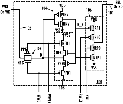
1. A latch bit cell of a static random access memory (SRAM) comprising:
a write portion of the latch bit cell, the write portion of the latch bit cell including,
an input node to receive data to be written to the write portion of the latch bit cell, wherein the data can be either a logical one or a logical zero;
a pass gate coupled to the input node and responsive to supply the data on the input node to a first node of the latch bit cell responsive to write word line signals being asserted;
an inverter coupled to the first node to supply inverted data;
a keeper circuit coupled to the inverter and configured to maintain the data on the first node when the write word line signals are deasserted and wherein an output of the keeper circuit is disabled responsive to the write word line signals being asserted during a write operation; and
a read portion of the latch bit cell coupled to receive read word line signals and responsive to assertion of the read word line signals to supply output data on an output node of the read portion of the latch bit cell, the output data corresponding to the data on the first node; and
wherein the read portion of the latch bit cell is formed by a first plurality of transistors having a first threshold voltage and the write portion of the latch bit cell, including the pass gate, the inverter, and the keeper circuit, is formed by a second plurality of transistors having a second threshold voltage, the second threshold voltage being higher than the first threshold voltage.
|