| CPC G09G 3/3233 (2013.01) [G09G 3/3208 (2013.01); H01L 29/7869 (2013.01); H01L 29/78651 (2013.01); H10K 59/126 (2023.02); H10K 59/131 (2023.02)] | 20 Claims |
|
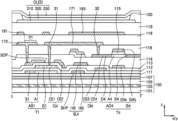
1. A display apparatus comprising:
a substrate comprising a display area including a display element;
a first thin film transistor disposed in the display area, the first thin film transistor comprising:
a first semiconductor layer including a silicon semiconductor; and
a first gate electrode insulated from the first semiconductor layer;
a second thin film transistor disposed in the display area, the second thin film transistor comprising:
a second semiconductor layer including an oxide semiconductor; and
a second gate electrode insulated from the second semiconductor layer;
a first signal line extending at a side of the first thin film transistor in a first direction;
a second signal line extending at an opposite side of the first thin film transistor in the first direction; and
a shielding pattern extending in the first direction, the shielding pattern at least partially overlapping the first signal line.
|