| CPC G06V 40/1318 (2022.01) [G02F 1/13338 (2013.01); G02F 1/133512 (2013.01); G02F 1/133526 (2013.01); G06F 3/042 (2013.01); G06V 40/1324 (2022.01); H01L 27/14621 (2013.01); H01L 27/14623 (2013.01); H01L 27/14627 (2013.01); H01L 27/14678 (2013.01); H10K 39/32 (2023.02); G02F 2201/56 (2013.01)] | 17 Claims |
|
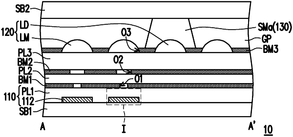
1. A fingerprint sensing device comprising:
a first substrate;
a sensing element layer located on the first substrate and comprising a plurality of sensing elements;
a second substrate located on the sensing element layer;
a micro-structure layer located between the second substrate and the sensing element layer, and comprising a plurality of micro-lens structures and a plurality of dummy structures, wherein orthogonal projections of the micro-lens structures on the first substrate respectively overlap orthogonal projections of the sensing elements on the first substrate; and
a spacer layer located between the second substrate and the sensing element layer, and comprising a plurality of main spacers, wherein each of the main spacers covers at least one of the dummy structures.
|