US 11,714,705 B2
Memory address protection circuit and method of operating same
Saman M. I. Adham, Hsinchu (TW); Ramin Shariat-Yazdi, Hsinchu (TW); and Shih-Lien Linus Lu, Hsinchu (TW)
Assigned to TAIWAN SEMICONDUCTOR MANUFACTURING COMPANY, LTD., Hsinchu (TW)
Filed by TAIWAN SEMICONDUCTOR MANUFACTURING COMPANY, LTD., Hsinchu (TW)
Filed on Jun. 30, 2022, as Appl. No. 17/855,412.
Application 17/855,412 is a continuation of application No. 16/989,018, filed on Aug. 10, 2020, granted, now 11,379,298.
Application 16/989,018 is a continuation of application No. 15/622,408, filed on Jun. 14, 2017, granted, now 10,740,174, issued on Aug. 11, 2020.
Claims priority of provisional application 62/427,684, filed on Nov. 29, 2016.
Prior Publication US 2022/0334916 A1, Oct. 20, 2022
This patent is subject to a terminal disclaimer.
Int. Cl. G06F 11/10 (2006.01); G06F 12/10 (2016.01); G06F 11/00 (2006.01); G06F 12/14 (2006.01)
CPC G06F 11/1016 (2013.01) [G06F 12/14 (2013.01); G06F 2212/1052 (2013.01)] 20 Claims
OG exemplary drawing
 
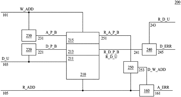
1. A memory circuit comprising:
a memory configured to store a data unit and parity bits, the parity bits including data parity bits based on the data unit and write address parity bits based on a write address associated with the stored data unit;
a write address port configured to receive the write address for the stored data unit;
a first decoding circuit configured to determine when a data error exists based on the stored data unit and the data parity bits;
a second decoding circuit configured to generate a decoded write address from a read address and the write address parity bits; and
an error detecting circuit configured to determine when an address error exists based on a comparison of the decoded write address to the read address.