| CPC G06F 9/3832 (2013.01) [G06F 9/3001 (2013.01); G06F 9/30181 (2013.01)] | 21 Claims |
|
1. A processing device, comprising:
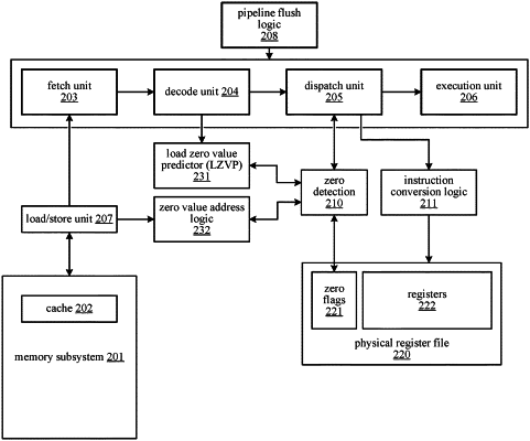
a zero value address logic circuit configured to, in response to detecting that a first instance of a load instruction is for storing a zero value, record a source address of the first instance of the load instruction;
a zero detection circuit configured to determine that an operand of a first instruction is zero based on the recorded source address; and
an instruction conversion logic circuit coupled with the zero detection circuit and configured to, in response to the zero detection circuit determining that the operand is zero, convert the first instruction to a register move instruction executable by the processing device.
|