| CPC G02B 6/4212 (2013.01) [G02B 6/122 (2013.01); G02B 6/124 (2013.01); G02B 6/13 (2013.01); G02B 6/132 (2013.01); G02B 6/30 (2013.01); G02B 6/34 (2013.01); G02B 6/3628 (2013.01); G02B 6/42 (2013.01)] | 15 Claims |
|
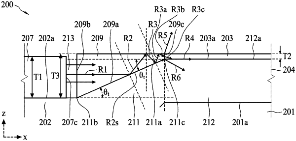
1. A device, comprising:
a waveguide;
a light coupling material disposed adjacent to the waveguide and having a first surface and a second surface opposite to the first surface, wherein a height of the first surface is less than a height of the second surface, and the waveguide is disposed more adjacent to the first surface than to the second surface;
a light emitting element, wherein the light coupling material is between the light emitting element and the waveguide, the light emitting element has a lateral surface facing the second surface of the light coupling material, and a height of the lateral surface of the light emitting element is substantially equal to the height of the second surface of the light coupling material from a cross-sectional view perspective.
|