|
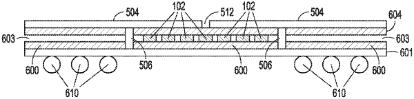
1. A printed circuit board (PCB) apparatus providing thermally matched first and second resistors using a thermal cage, the PCB apparatus comprising: a first resistor PCB layer, including the first resistor, the first resistor PCB layer having a first side and an opposing second side; a second resistor PCB layer, including the second resistor, the second resistor PCB layer having a third side and an opposing fourth side, the second resistor PCB layer located above the second side of the first resistor PCB layer with the third side of the second resistor PCB layer facing toward the second side of the first resistor PCB layer; a thermal conduction PCB layer, having a fifth side and an opposing sixth side, the thermal conduction PCB layer located above the fourth side of the second resistor PCB layer, with the fifth side of the thermal conduction PCB layer facing toward the fourth side of the second resistor PCB layer, the thermal conduction PCB layer being more thermally conductive than the first and second resistor PCB layers; and an electrically insulating gap that divides the thermal conduction PCB layer into first and second regions to avoid electrically shorting either or both of the first resistor layer or the second resistor layer through the thermal conduction PCB layer.
|