US 11,713,518 B2
Method for forming chalcogenide thin film
Unyong Jeong, Pohang-si (KR); Giri Anupam, Pohang-si (KR); Geonwoo Kim, Pohang-si (KR); and Ghorai Arup, Pohang-si (KR)
Assigned to POSTECH RESEARCH AND BUSINESS DEVELOPMENT FOUNDATION, Gyeonsangbuk-Do (KR)
Filed by POSTECH Research and Business Development Foundation, Pohang-Si (KR)
Filed on Jan. 5, 2022, as Appl. No. 17/569,098.
Claims priority of application No. 10-2021-0001456 (KR), filed on Jan. 6, 2021; application No. 10-2021-0001519 (KR), filed on Jan. 6, 2021; and application No. 10-2022-0000830 (KR), filed on Jan. 4, 2022.
Prior Publication US 2022/0213619 A1, Jul. 7, 2022
Int. Cl. C30B 7/14 (2006.01); C30B 29/46 (2006.01); C30B 30/04 (2006.01); H01L 21/02 (2006.01)
CPC C30B 29/46 (2013.01) [C30B 7/14 (2013.01); C30B 30/04 (2013.01); H01L 21/02293 (2013.01); H01L 21/02422 (2013.01)] 18 Claims
OG exemplary drawing
 
1. A method for forming a chalcogenide thin film, the method comprising:
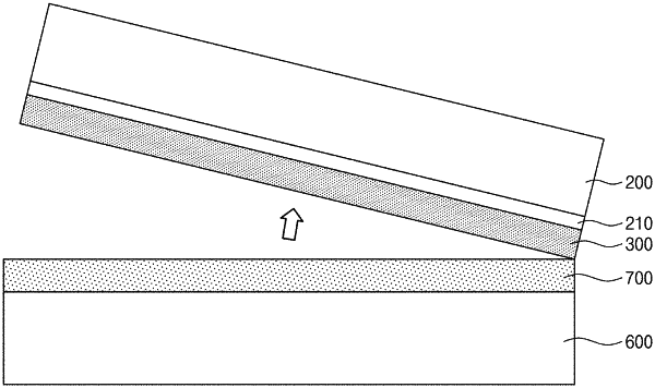
forming a chalcogen element-containing film on a carrier substrate;
disposing the chalcogen element-containing film on a silicon wafer, wherein a surface of the silicon wafer and a surface of the chalcogen element-containing film are in contact with each other;
performing heat treatment on the silicon wafer and the chalcogen element-containing film at least one time; and
removing the carrier substrate,
wherein the silicon wafer has a crystal plane of (111).