| CPC C23C 16/45553 (2013.01) [C23C 16/36 (2013.01); C23C 16/45542 (2013.01); H01L 21/0228 (2013.01); H01L 21/02126 (2013.01); H01L 21/02219 (2013.01); H01L 21/02274 (2013.01); H01L 29/78 (2013.01)] | 7 Claims |
|
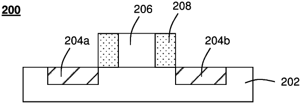
1. An electronic device comprising:
a substrate having an active region with at least one gate stack formed thereon, the at least one gate stack having a first side and a second side;
a source material;
a drain material; and
a spacer material on the first side and on the second side of the gate stack, the spacer material comprising one or more of a silicon oxycarbide (SiOC) film and a silicon oxycarbonitride (SiOCN) film, the silicon oxycarbide (SiOC) film and the silicon oxycarbonitride (SiOCN) film substantially free of amorphous carbon.
|